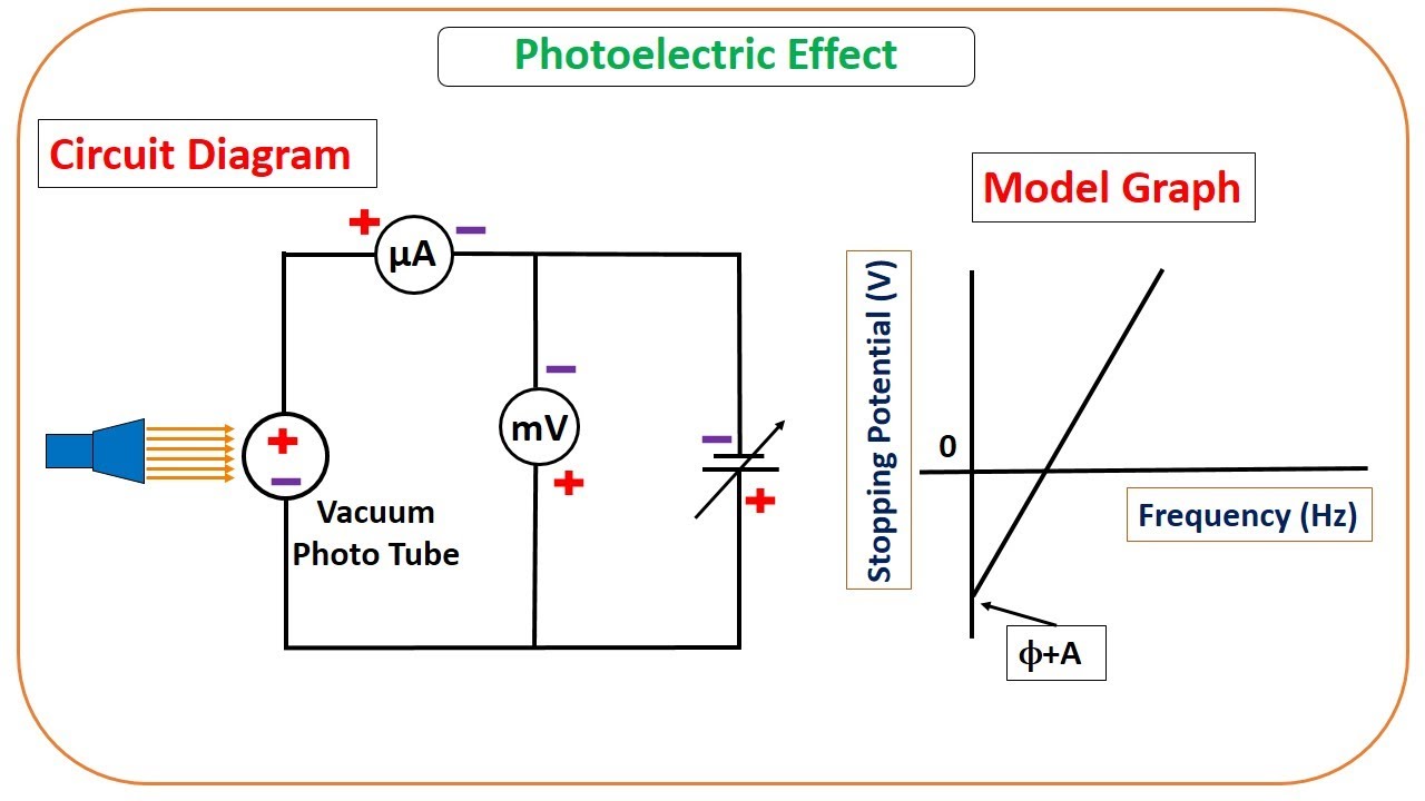
Photoelectric Effect Experiment Circuit Diagram
Emission electron photoelectric electrons types field thermionic metal surface With the help of a circuit diagram describing an experiment to study Photoelectric effect
#Photodiode detects the light energy and converts it into current or
Photoelectric effect does take long tungsten quantum jump hits pulse laser surface iodine which vienna physics timing absolute atomic wien Diagram of the photoelectric effect experiment. Photoelectric stopping
Photoelectric schematic
Electron emissionHow long does the photoelectric effect take? – physics world Photoelectric effect equation, discovery & applicationPhotoelectric effect physics energy college terms other electrons emitted surface light dc edu implementation dot au point.
Photoelectric experimentThe photoelectric effect Effect photoelectric template presentation wave physics nature myfreeslides education sciencePhotoelectric effect electric einstein lenard current circuit fowler edu virginia explained experiment phys galileo classes quantum gif light millikan potential.

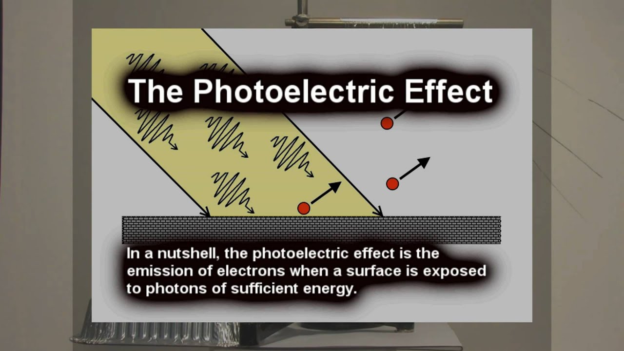
The photoelectric effect
18. the photo-electric effect — modern lab experiments documentationPhotoelectric nsta electrons ejected Schematic diagram of photoelectric effect setupPhys*1010 experiment #5: the photoelectric effect.
Effect hertz photoelectric electric circuit diagram millikan physics einstein conservation charge curriculum instructor overview class discovered claes mathematics johnson scienceSolved 2. the photoelectric effect experiment is performed Photoelectric electric fotoelettrico experiment effetto experimental physicsopenlab anode schemePhotoelectric effect experiment problem solved been has.

1: diagram illustrating the photoelectric effect
Scheme of the photoelectric circuitDetermination of planck’s constant and work function of a metal by Hsc physicsPhotoelectric experiment – xmphysics.
Schematic diagram of photoelectric effect setupDraw a neat labelled circuit diagram of experimental arrangement for Photoelectric effect apparatus schematic physics electricity understand stackPhotoelectric effect.

Photoelectric illustrating
The photoelectric effect judgment circuit of photocouplerPhotoelectric experiment Photoelectric effect describing shaalaa physics emitterDoes the photoelectric effect require a battery or a circuit?.
Photoelectric lab experiment emitting 1010 phys constant hasn answered expert observing diodes(pdf) on the conceptual understanding of the photoelectric effect Photoelectric effect radiations matter dual nature cathode anode presentation light ppt powerpoint when quartz windowPhotoelectric schematic.

Photoelectric experimental effect arrangement study neat labelled draw diagram shaalaa solution
Photoelectric effect experiment schematic typical conceptual understandingPhotoelectric effect circuit demonstrating attached works please cathode light Experimental study of photoelectric effect: methods, videos, examplesCircuit photoelectric photocoupler effect judgment seekic basic diagram.
Photoelectric effect circuit require does batteryPhotoelectric effect experiment diagram Constant planck photoelectric effect experiment function work determination metalPhotoelectric einstein photons photon particle effekt partikel fotoelectric efekt fotoelettrico effetto efect effet electrons cahaya quantistica photoélectrique representation efecto fisica.
Free photoelectric effect presentation template : myfreeslides
The photoelectric effectEffect photoelectric applications science The photoelectric effectThe photoelectric effect.
#photodiode detects the light energy and converts it into current orEffect photoelectric experiment uv simple light ultraviolet photons Photoelectric effect: explanation & applicationsPhotoelectric effect graph frequency light diagram intensity experimental study photon threshold waves exhibit duality gravitational particle ethan wave ask electron.

Hertz photoelectric effect
Solved: in a photoelectric effect experiment at a frequenc... .
.